
Appearance
Model Training: Find Missing Pieces in Circuit Boards
Overview
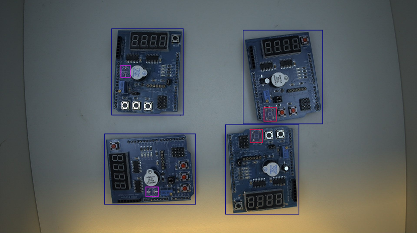
In this tutorial, you will set up all necessary components and train an AI model to detect missing components on printed circuit boards (PCBs).
Estimated time
60–75 minutes.
What you'll learn
- Prepare and upload image datasets for training and validation.
- Add and manage annotations for object detection tasks.
- Configure a model training workspace and problem.
- Train an object detection model using a predefined architecture.
What you'll build
By the end of this tutorial, you'll have a trained object detection model capable of identifying missing components on PCB images. This model can later be deployed and integrated into inspection workflows.
Prerequisites
To complete this tutorial, you will need the following:
- The password for the
platformadminuser, which you received via email when you installed the platform. - A machine with a GPU that has at least 8 GB of VRAM.
- Downloaded training dataset, training annotations, validation dataset, validation annotations.
To complete this tutorial, you need the platformadmin role. If you don't have this role, you cannot access model training.
Step 1: Create a Training and Validation Dataset
In the Hub, go to the Dataset tab and create two image datasets using the files from the prerequisites section. Name the first dataset PCB Train (PCB_train_1920x1080_dataset.zip) and the second dataset PCB Val (PCB_val_1920x1080_dataset.zip). If you don't know how to create a dataset, go to Create an Image Dataset and then come back.
Step 2: Add Annotations to Your Datasets
To train a model, you also need to provide annotations.
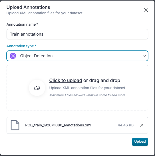
- Click the
Add Annotationsbutton next toUpload files. - Name it
Train annotations, chooseObject Detectionfrom theAnnotation typemenu, and drag and drop the provided training annotations file (PCB_train_1920x1080_annotations.xml). - Click
Upload.
- Repeat the process for the validation dataset using the corresponding annotation file and name.
Step 3: Create a Model Training Workspace
In the left navigation, switch from the Datasets tab to the Model Training tab.
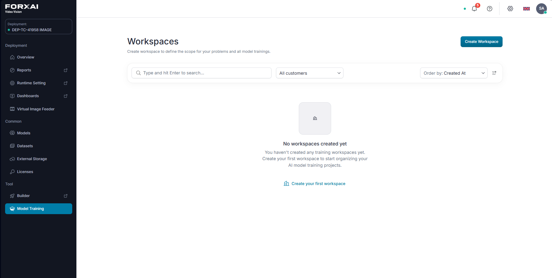
- Click
Create Workspacein the top right. - In the
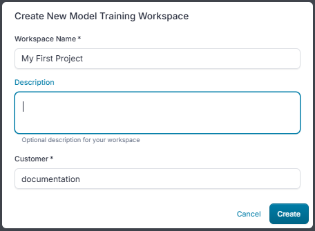
Create New Model Training Workspacepopup:- Name it
My First Project. - Enter
documentationin the customer field. - Optionally add a description.
- Name it
- Click
Create.
Step 4: Create a Problem
Within a workspace, you can define multiple problems.
- In the header of
My First Project, clickCreate Problem. - In the popup: Name the problem
PCB Missing Components. - Click
Create.
Step 5: Prepare Training Configuration
You will now configure the training using the stepper interface. Follow the instructions for each step and proceed using the Next button.
- Basic configuration
- Name:
PCB object detection. - Problem Type:
Object Detection. - Model Architecture:
Faster R-CNN.
- Name:
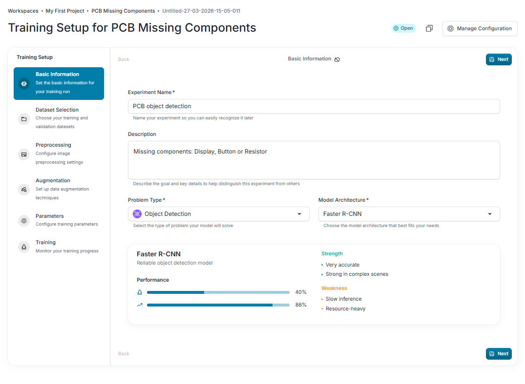
- Datasets and annotations
- Training dataset:
PCB Train. - Training annotations:
Train annotations. - Validation dataset:
PCB Val. - Validation annotations: corresponding validation annotations.
- Training dataset:
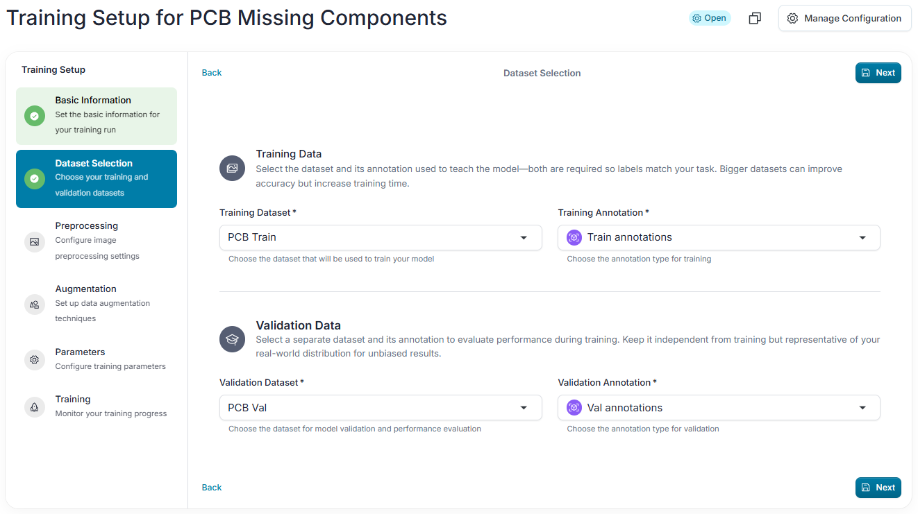
- Preprocessing
- Set image resolution to
1440x810to reduce computational load.
- Set image resolution to
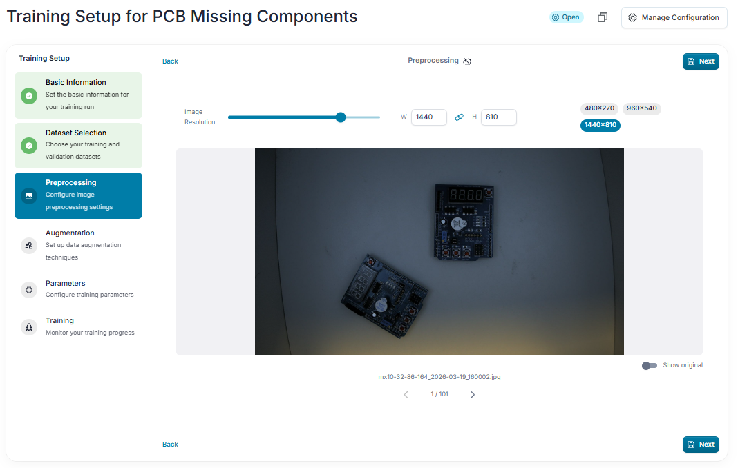
Data augmentation
- Add
Random Color Adjustmentaugmentation. - Keep the default settings.
- Add
💡 Augmentaions improve robustness.
Training works also without the Random Color Adjustment augmentation, but adding it improves robustness, especially to lighting changes and small color variations between boards.
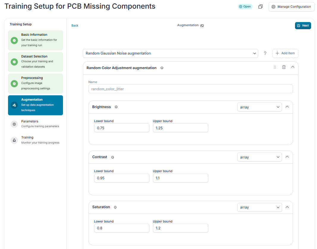
- Training configuration
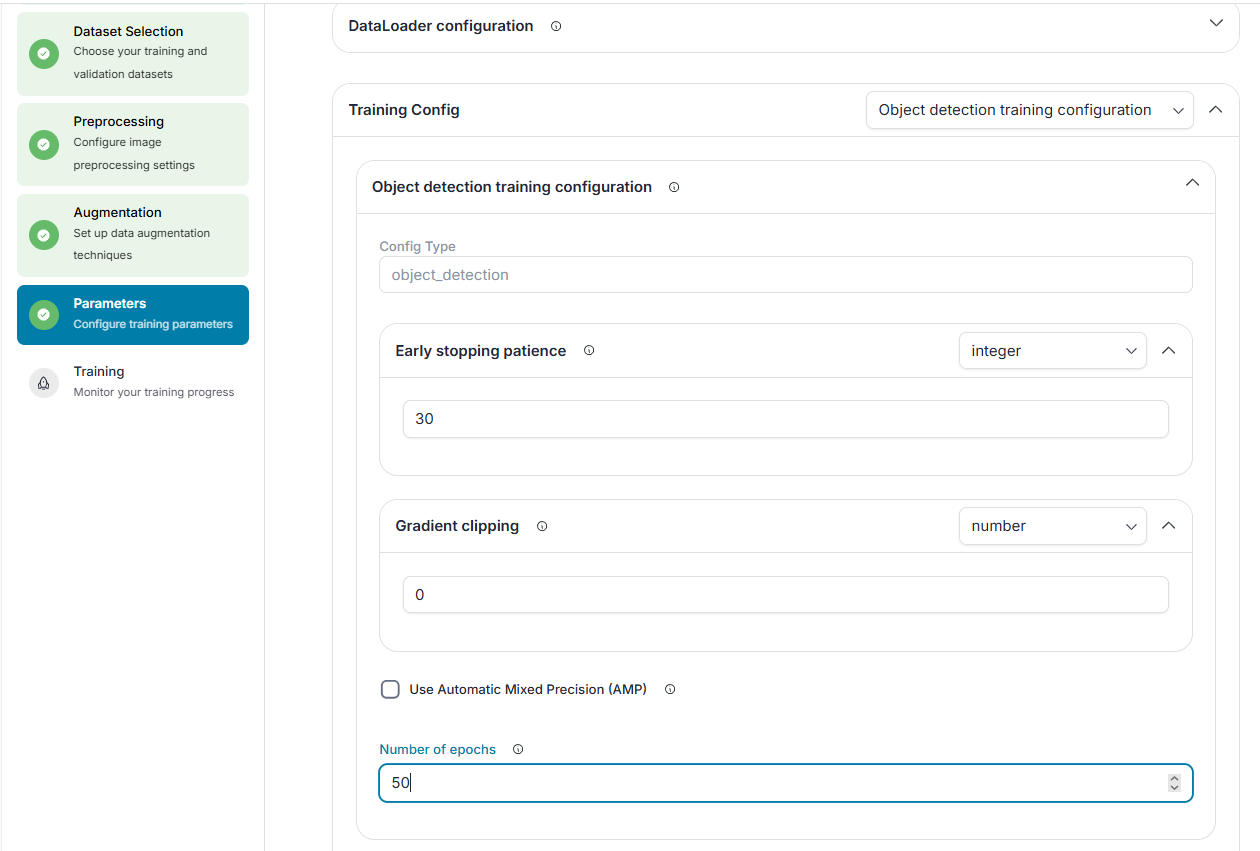
- Open
Object detection training configuration. - Set
Number of epochsto50. - Leave all other settings as default.
- Open
- Start training
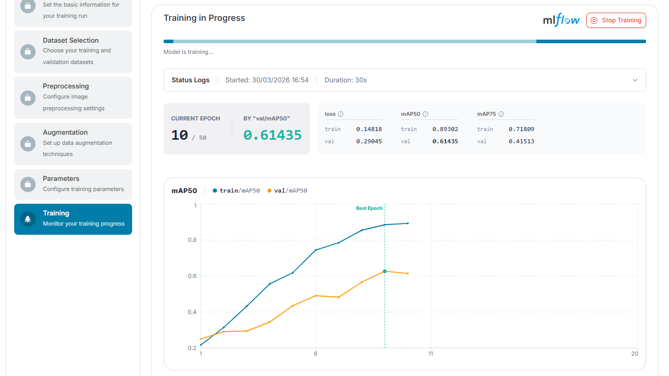
- Click
Start Training. - Monitor the live training metrics.
- Click
Now you have completed model training.
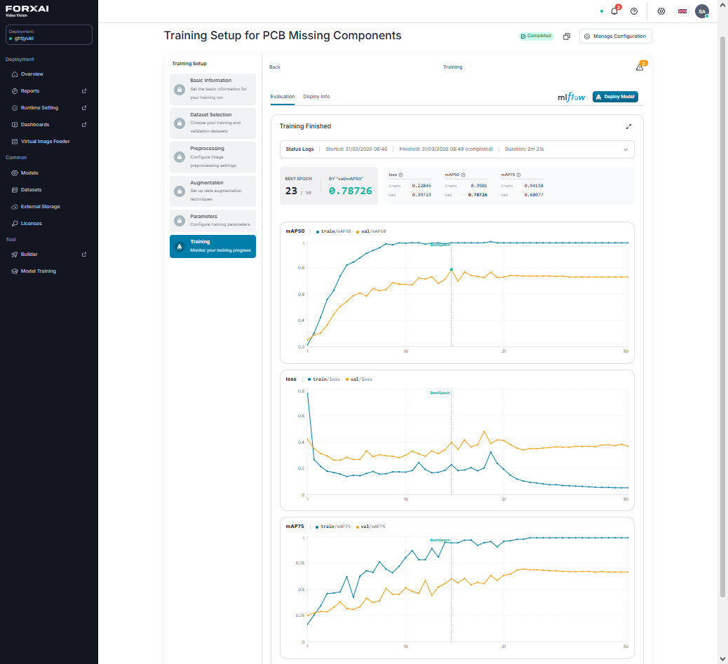
⚠️ Training results may vary.
Training is not fully deterministic due to data ordering, augmentation, and slight variations in numeric operations. This can change exact mAP values, but overall results remain consistent.
Next steps
Now that you've completed this tutorial, you can learn how to: